Welcome to Edinburgh Instruments’ blog celebrating our work in Raman, Photoluminescence, and Fluorescence Lifetime Imaging. Every month, we aim to highlight our pick for Map of the Month to show how our Raman and fluorescence spectrometers can be used to reveal all the hidden secrets in your samples.

To obtain high-quality optoelectronic devices containing GaN, manufacturers must ensure minimal mechanical and electrical heterogeneity caused by stress-induced crystalline deformations. These can cause changes in the bandgap and charge carrier mobility of the material and can significantly reduce the properties of the material.
Non-destructive analytical techniques sensitive to these phenomena, of which Raman spectroscopy is an excellent example, are therefore essential to monitor GaN during manufacturing. As will be shown, it is sensitive to even the most subtle changes in the material and when coupled to a microscope, the spatial resolution of different stress and crystallinity states within the material is possible.
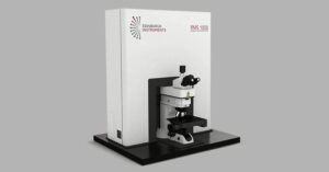
In our recent Application Note, we showed how the Edinburgh Instruments RMS1000 Confocal Microscope can be used to perform Raman and PL imaging on a GaN-based LED device, a picture of which is shown in panel (a) above. In this Map of the Month, we highlight the information provided about the LED by Raman imaging.
An area of the GaN chip was imaged using spectral mapping with a 638 nm laser. To determine the distribution of GaN within this area, the intensity of the E2 (high) mode was imaged, Figure 4b.
The position of the E2 (high) was imaged and is shown in panel (c). The Raman shift of this mode can be correlated with strain in GaN, with an increase in Raman shift relative to 567 cm-1 showing compressive strain and a decrease showing tensile strain, respectively. The image below shows how tensile and compressive strain affect bond lengths and atomic positions within a lattice. Raman microscopy can readily visualise strain on semiconductor materials such as GaN and silicon.
In the image in panel (c), yellow and red regions indicate areas where the GaN is experiencing compressive strain, and the black regions represent areas of tensile strain. The spectra in panel (d) show the variation in intensity and peak position of the GaN E2 band across the images.

Read our full Application Note to find out more about how Raman and PL microscopy were used to analyse this GaN-based LED.


