Gallium nitride (GaN) has emerged as a leading material in the semiconductor industry, offering significant advantages over traditional silicon-based technologies. GaN is a binary III/V semiconductor with a direct bandgap of around 3.4 eV, which is over three times that of silicon (1.1 eV).1,2 This wide bandgap allows GaN to withstand high electric fields, leading to smaller and more efficient power electronics used for processing high voltages and currents.
The large bandgap of GaN leads to electroluminescence emission of near-UV to blue light, making GaN extremely useful for UV and blue light-emitting diodes (LEDs) and lasers.3 Other useful properties of GaN include its durability, high conductivity and high heat capacity. These make GaN an ideal candidate for use in transistors used in high-voltage and high-temperature applications such as wireless communication infrastructure and aerospace technologies.
It is important to ensure GaN materials are high quality with minimal mechanical and electrical heterogeneity caused by strain and crystal defects. Photoluminescence (PL) offers a sensitive, non-destructive technique for assessing the quality of GaN materials. When defects are present in the material, defect-induced energy levels with lower bandgaps are formed causing the emission of radiation of different wavelengths.4 Common defects in GaN produce luminescence in the yellow range.
Time-resolved PL measurements provide additional insight into the quality of GaN materials. GaN exhibits very fast PL lifetimes in the picosecond to nanosecond range. In contrast, defects typically exhibit longer lifetimes in the microsecond to second range.4
This Application Note demonstrates the use of an Edinburgh Instruments FLS1000 Photoluminescence Spectrometer coupled to an external picosecond pulsed UV laser to perform both steady-state and time-resolved PL measurements of GaN.
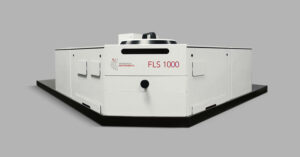
Measurements were performed using an FLS1000 equipped with an externally coupled 266 nm picosecond pulsed laser (PS-D-266_Air_A_10mW, CNI Laser) and a high-speed hybrid-PMT detector (HS-HPD) (Figure 1).
The analysed sample was undoped n-type GaN on a sapphire substrate manufactured using the halide vapour phase epitaxy (HVPE) growth method. The sample was placed in a front-face sample holder, and the setup included a 325 nm longpass filter placed before the emission monochromator to eliminate laser scattering as the sample was reflective.
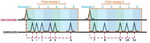
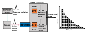
Time-resolved PL measurements of GaN were collected using time-correlated single photon counting (TCSPC) with a laser repetition rate of 500 kHz. The GaN defects were identified using multichannel scaling (MCS) with a microsecond xenon flashlamp at a 100 Hz repetition rate.
Figure 1. FLS1000 spectrometer with an externally coupled 266 nm laser, front-facing sample holder, and hybrid PMT detector used for PL measurements of GaN.
PL spectroscopy is a useful approach for determining energy gaps, particularly in wide bandgap semiconductors such as GaN. The emission spectrum of GaN, shown in Figure 2, exhibits a peak at 365 nm corresponding to a bandgap energy of 3.4 eV. This peak originates from the band-edge emission of GaN, resulting from the direct band-to-band recombination between electrons in the conduction band and holes in the valence band.
In addition, a broader luminescence band at around 550 nm (2.25 eV) was observed corresponding to defect-related emission in the GaN. This defect luminescence in the material is often attributed to gallium vacancy-related defects.
Figure 2. Emission spectrum of GaN. Measurement parameters: λex = 266 nm, Δλem = 1 nm, step = 0.5 nm, dwell time = 1 s.
PL Lifetimes were collected at 370 nm and 550 nm emission to evaluate GaN and defects, respectively. The PL lifetime of the GaN band-edge emission at 370 nm was measured using TCSPC. The instrument response function (IRF) was measured at the laser wavelength (266 nm). The fluorescent decay, IRF and calculated lifetime are shown in Figure 3.
Figure 3. Fluorescence decay and calculated PL lifetime of GaN at 370 nm emission. Measurement parameters: λex = 266 nm, Δλem = 1 nm, repetition rate = 500 kHz.
The decay was fitted as a reconvolution of the IRF and the exponential decay of the sample. The photoluminescence decay was fitted with a three-component exponential giving relaxation times of 0.26, 0.77 and 5.78 ns. This yielded an intensity average lifetime of 1.11 ns.
The PL lifetime of the defect emission at 550 nm was also measured using MCS single photon counting and a microsecond xenon flashlamp excitation source (Figure 4).
Figure 4. Fluorescence decay and calculated PL lifetime of GaN at 550 nm emission. Measurement parameters: λex = 365 nm, Δλex = 1 nm, Δλem = 3 nm, repetition rate = 100 Hz.
The decay was fitted using a three-component exponential giving relaxation times of 141.2, 915.2 and 2906.8 µs, resulting in an intensity average lifetime of 2.22 ms. The longer lifetime in the range of microsecond to second was characteristic of defects in GaN, demonstrating that this technique was effective for assessing the quality of GaN materials.
The FLS1000 spectrometer coupled with an external UV laser allowed measurement of steady state and time-resolved PL of GaN. The steady state PL spectrum showed emission bands typical of crystalline GaN and GaN with structural defects. Time-resolved PL measurements of these emission bands confirmed this. The combination of steady state and time-resolved PL analysis is an effective tool for characterising the quality of GaN.