Gallium nitride (GaN) is a binary III/V semiconductor that has earned a reputation as a potential successor to silicon. GaN has a wider bandgap than silicon, which means it can sustain higher voltages in electronic devices.1 Higher voltages allow for the design of smaller and more energy-efficient GaN components than is practical with silicon. GaN also outperforms silicon when operating at high temperatures, which could ease current design constraints imposed by silicon technology in complex or demanding environments such as automobile electronics.2 GaN is also used extensively in the photonics industry and is the material responsible for UV and blue light-emitting diodes (LEDs) and lasers, the discovery of which paved the way for energy-efficient white LED lighting and resulted in the 2014 Nobel Prize in Physics being awarded to Shuji Nakamura, Akasaki Isamu, and Amano Hiroshi.
To obtain high-quality optoelectronic devices containing GaN, manufacturers must ensure minimal mechanical and electrical heterogeneity caused by strain and crystal defects. Non-destructive analytical techniques sensitive to these phenomena, of which Raman and photoluminescence (PL) are examples, are therefore essential to monitor GaN during manufacturing. This Application Note demonstrates Raman and PL characterisation and imaging of a GaN device using an Edinburgh Instruments RMS1000 Confocal Microscope. It is shown that both optical techniques are sensitive to even the most subtle changes in the material and that when coupled to a microscope, the spatial resolution of different states within the material is possible.
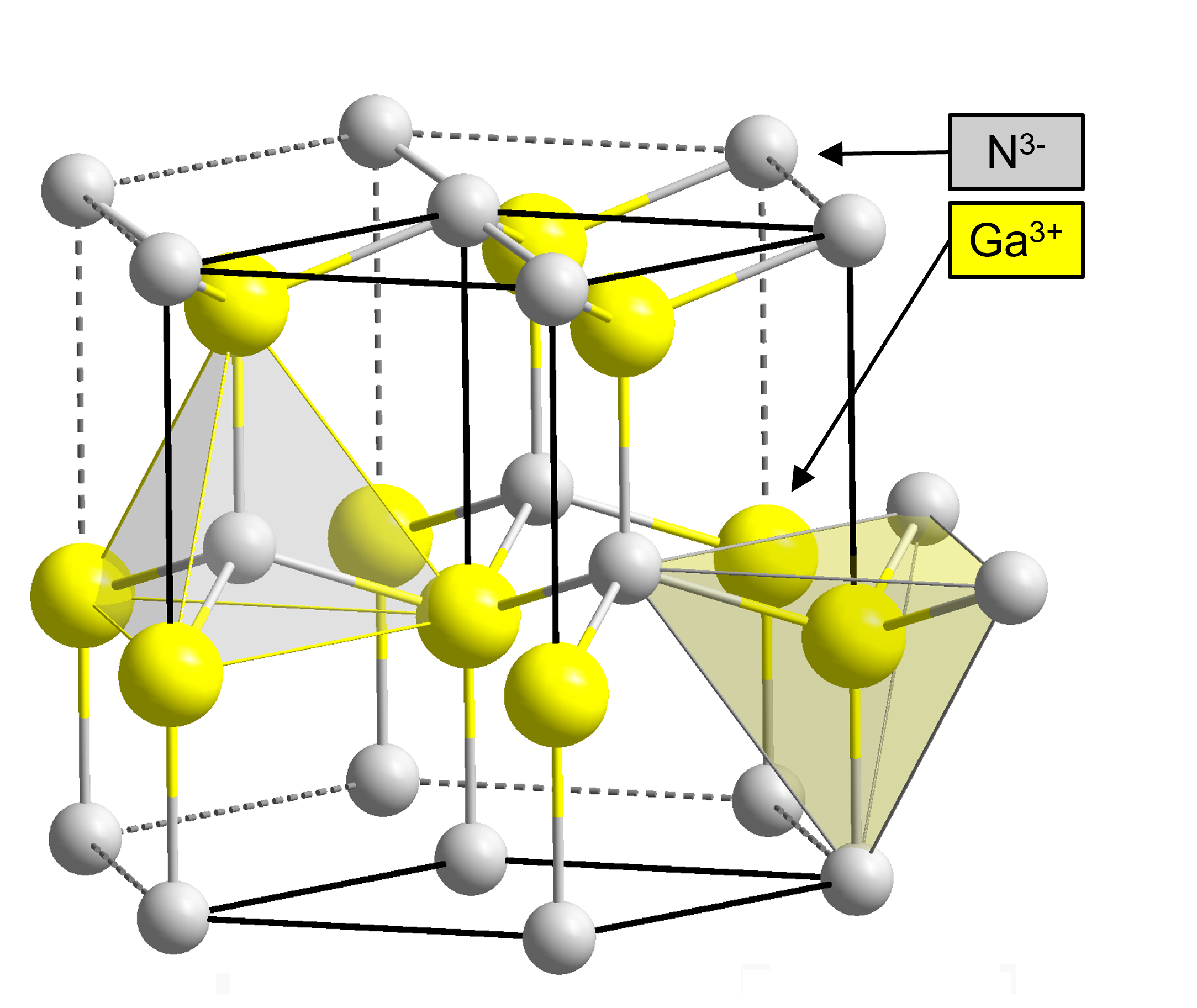
Figure 1. GaN Wurtzite crystal structure with the unit cell shaded yellow.
The samples analysed were LED chips on an adhesive film produced by EPIGAP Optronic GmbH designed to emit at 520 nm. The LEDs consisted of GaN-based layers grown epitaxially on sapphire and Au alloy bonding pad electrodes. An RMS1000 was equipped with an externally coupled 325 nm He-Cd laser for PL characterisation, a 638 nm laser for Raman characterisation, and a CCD camera in a 225 mm spectrograph, Figure 2. A 40X 0.47 NA UV objective lens was used when probing the sample with the 325 nm laser, and a 100X 0.9 NA objective lens was used for the 638 nm analysis. An automated X, Y and Z-stage allowed for imaging with both spectroscopic techniques.
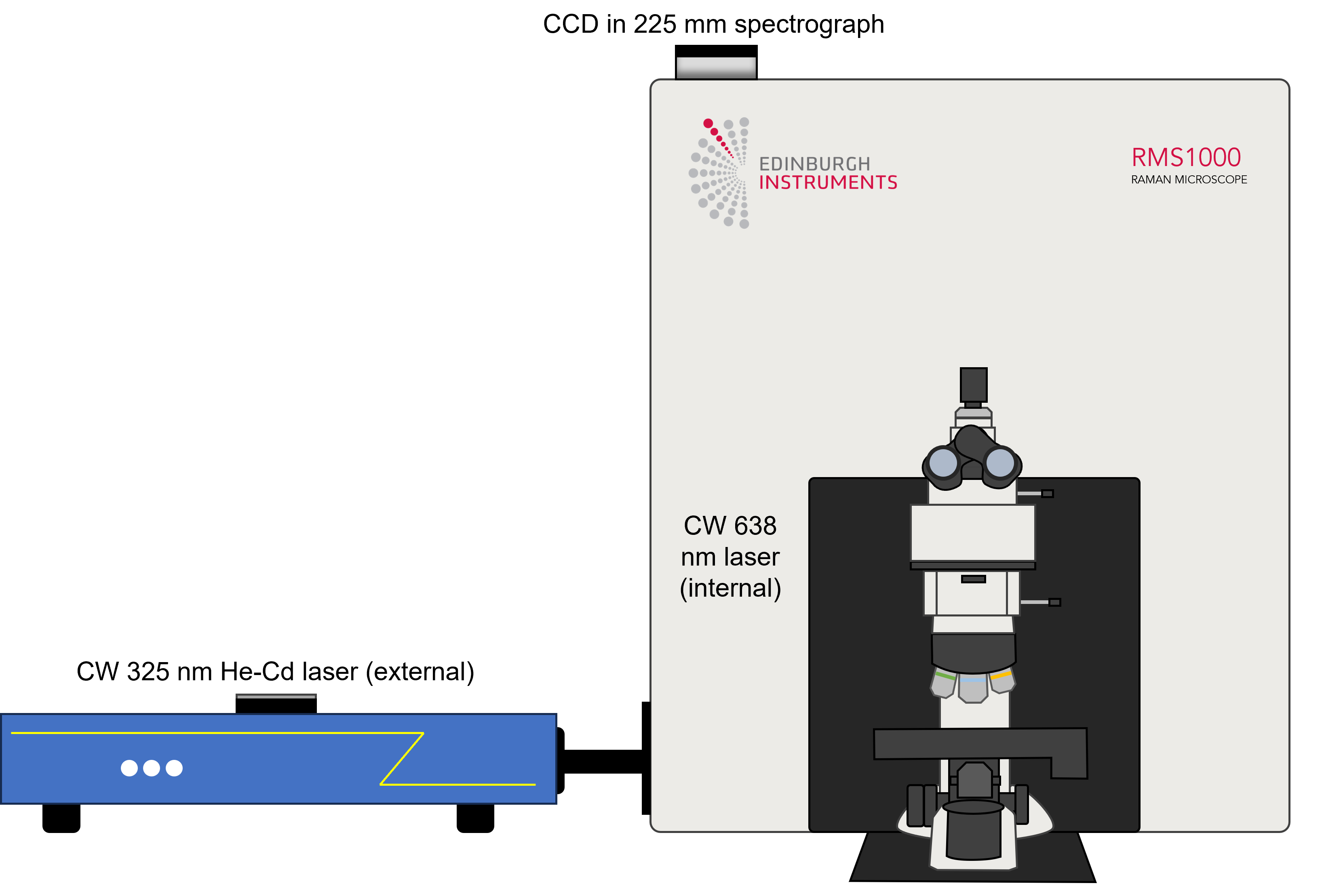
Figure 2. RMS1000 Confocal Microscope used for PL and Raman characterisation of GaN.
Firstly, the GaN LED chip was investigated using Raman microscopy. In the Raman spectrum in Figure 3, the two main bands for GaN are shown in red. These are the E2 band at 567 cm-1 and the A1 longitudinal optical (LO) phonon at 735 cm-1.3 A peak at 670 cm-1 was also observed, previously attributed by Cardoso et al. as a disorder-activated vibrational mode of GaN.4 Also observed were Raman bands from the underlying sapphire substrate (Al2O3) at 420 cm-1 and 750 cm-1. The typical PL signature from Cr3+ doped Al2O3 was observed ca. 1300 cm-1, corresponding to approximately 1.786 eV (694 nm).5
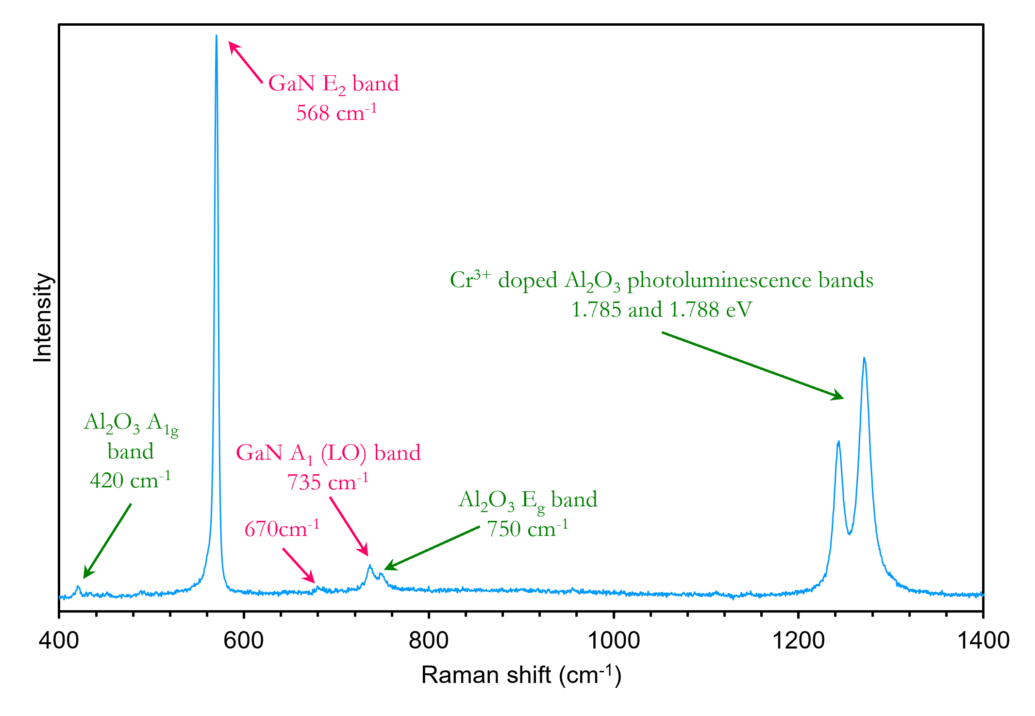
Figure 3. Raman spectrum of GaN.
An area of the GaN chip was imaged using spectral mapping with the 638 nm laser, . To determine the distribution of GaN within this area, the intensity of the E2 (high) mode was imaged, Figure 4b. It can be observed that the intensity was consistently higher in the region of the chip within the P- and N-GaN layers. The position of the E2 (high) mode was also mapped, Figure 4c. The Raman shift of this mode can be correlated with strain in GaN, with an increase in Raman shift relative to 567 cm-1 showing compressive strain and a decrease showing tensile strain, respectively. Raman microscopy can readily visualise strain on semiconductor materials such as GaN and silicon. In the image in Figure 4c, yellow and red regions indicate areas where the GaN is experiencing compressive strain, and the black regions represent areas of tensile strain. The spectra in Figure 4d show the variation in intensity and peak position of the GaN E2 band across the images. The sapphire PL intensity was also imaged in Figure 4e, with corresponding spectra in Figure 4f, showing that the sapphire PL was diminished in the areas with the highest GaN Raman intensity.
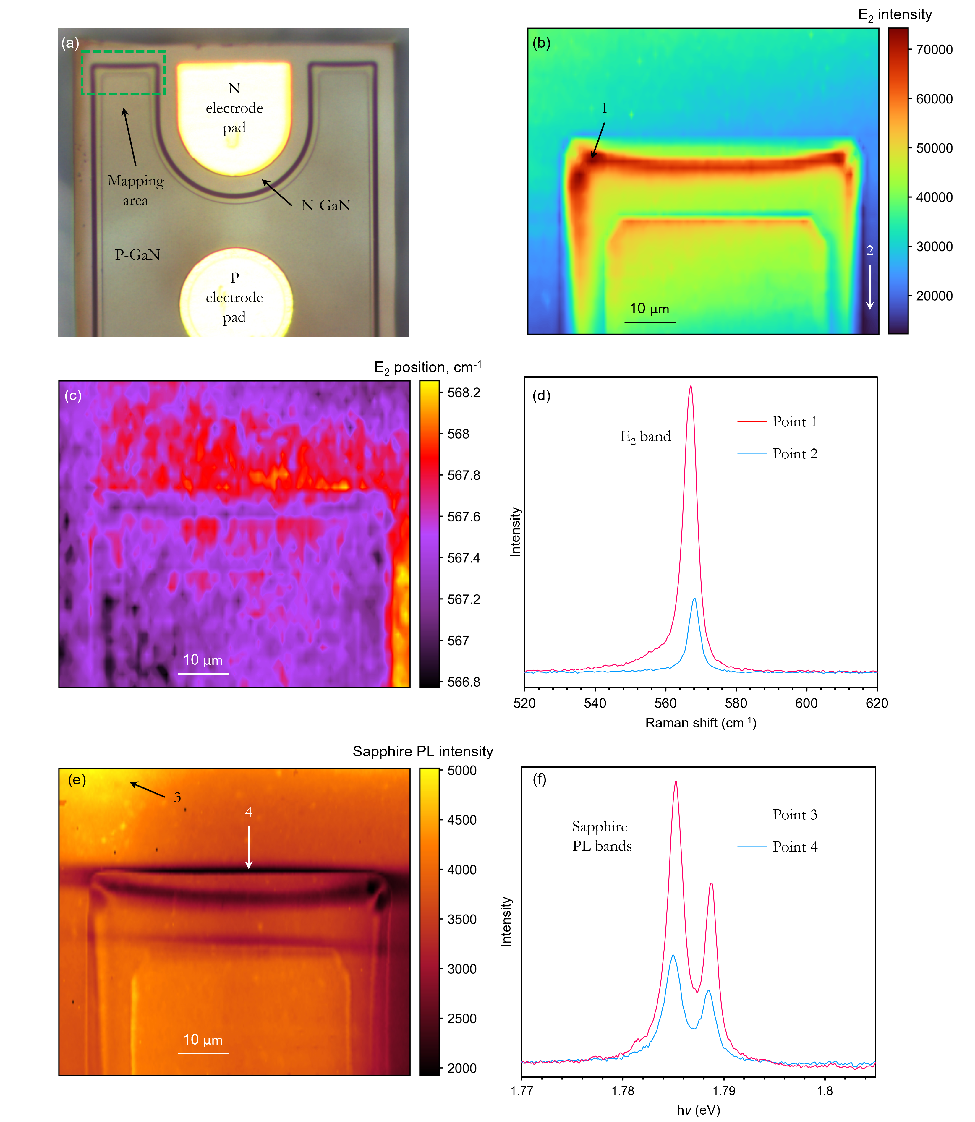
Figure 4: Raman mapping of GaN.
The GaN chip was also analysed using PL microscopy. PL directly measures bandgaps in semiconductor materials, and since bandgap energies are highly sensitive to impurities such as dopants and defects, microscopic analysis of devices can yield information about their presence. The PL spectrum of GaN, Figure 5, at room temperature, is dominated by a strong near-band-edge (NBE) emission at 3.41 eV (364 nm), which correlates to the direct band-to-band recombination between electrons in the conduction band and holes in the valence band, Figure 4.6 To excite and observe this band, a 325 nm He-Cd laser was externally coupled to the RMS1000. Also observed in the spectrum were PL bands at 2.33 eV (532 nm) and 1.71 eV (725 nm). The sapphire PL band was not observed, which was attributed to the higher absorption coefficient of the surface GaN material when the 325 nm UV excitation wavelength was used.
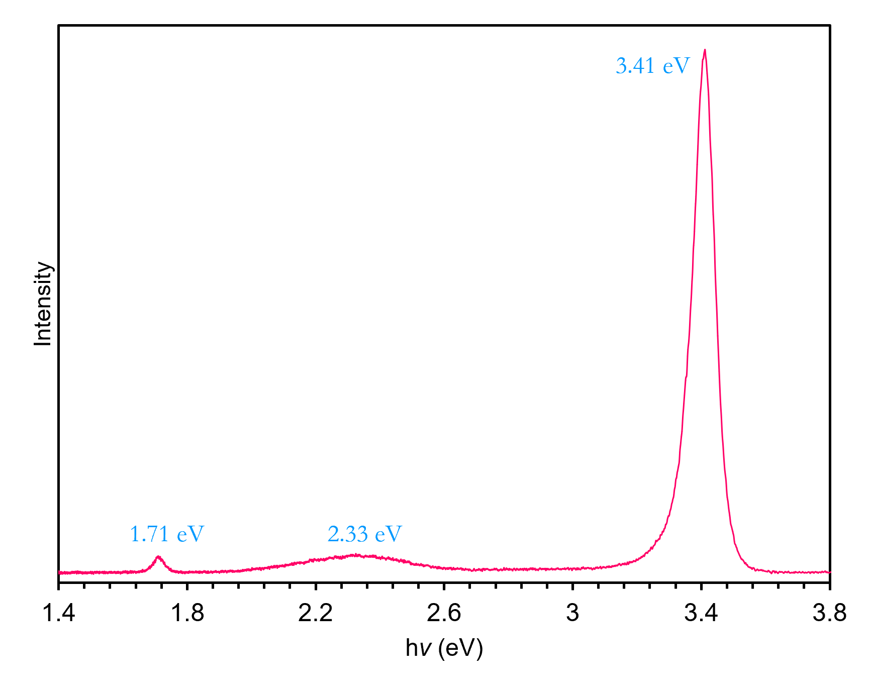
Figure 5. Photoluminescence spectrum of GaN.
PL imaging was conducted on the same part of the chip investigated using Raman, Figure 6. The entire region shown in Figure 6a visualised in brightfield through the UV objective, was investigated, and false colour imaging was performed using UV and visible bands, Figures 6b and c. The 3.41 eV NBE UV PL intensity image shows that the P-GaN region of the chip does not exhibit PL. The effect of diminishing NBE PL of GaN with increasing Mg dopant concentration (P doping) was previously reported in a study by Hess et al.7 The N-GaN region emits UV PL strongly, except for a region in the top right-hand side of the image, shown in the Raman image in Figure 4c to be experiencing compressive strain.
The chip also emitted at 2.38 eV (520 nm), which corresponds to the PL from InGaN; the layer sandwiched between P- and N-GaN that gives the LED its green colour. The emission in this region was more intense and blue-shifted from the weak visible emissions in the N-GaN layer. This emission was largely confined to the black strip at the boundary of the P and N layers. The UV and green PL spectra from points 1 and 2 on both maps are shown in Figure 6d.
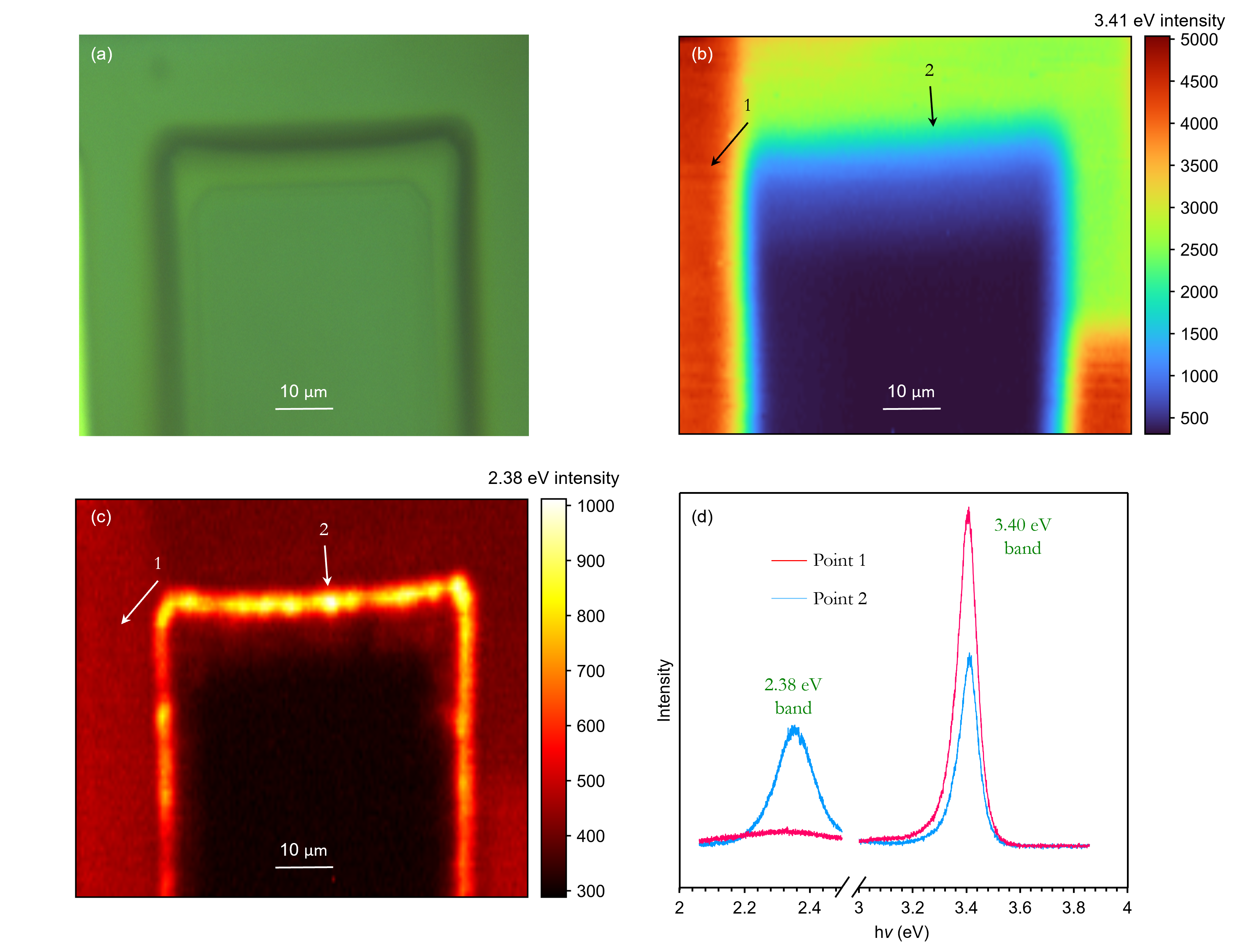
Figure 6. PL mapping of GaN.
The RMS1000 Raman and PL Confocal Microscope is ideal for the analysis and characterisation of GaN-based devices. The combination of the Raman and PL techniques allowed for the visualisation of differences in the crystalline structure and chemical composition of the constituent materials across the chip. These two techniques are extremely useful for the non-destructive quality control monitoring of GaN-based devices.